PROBLEM STATEMENT
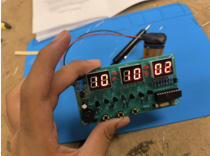
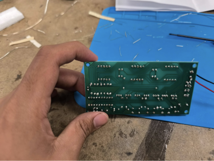
Assemble and test a fully functional digital electronic clock by populating a pre etched PCB with through hole components, executing high quality solder joints for reliable electrical connectivity, and verifying correct operation through power on and functional testing. The build should demonstrate correct component identification and placement, proper soldering technique that avoids cold joints and solder bridges, and successful validation of timekeeping accuracy, display readability, and switch responsiveness.
BILL OF MATERIALS
| Item | Qty | Specification / designators | Purpose |
|---|---|---|---|
| Pre etched printed circuit board (PCB) | 1 | PCB | Base board for the clock circuit |
| Resistors | set | R1 to R18 | Biasing and current limiting |
| Capacitors | set | C1 to C6 | Timing, filtering, and stability |
| Quartz crystal oscillator | 1 | Y1 | Time base reference |
| Integrated circuits | set | U1 to U3 | Control and logic for clock operation |
| Diodes | set | D1 to D4 | Rectification and protection as required |
| Seven segment displays | 3 | DS1 to DS3 | Visual time display output |
| Transistors | set | Q1 to Q7 | Switching and driving loads |
| Connectors | set | CJ01 to CJ03 | External connections and interfacing |
| Push button switches | 3 | S1 to S3 | User input controls |
| Solder wire | as needed | solder wire | Electrical and mechanical joints |
| Flux | as needed | flux | Improves solder wetting and joint quality |
IMAGES