


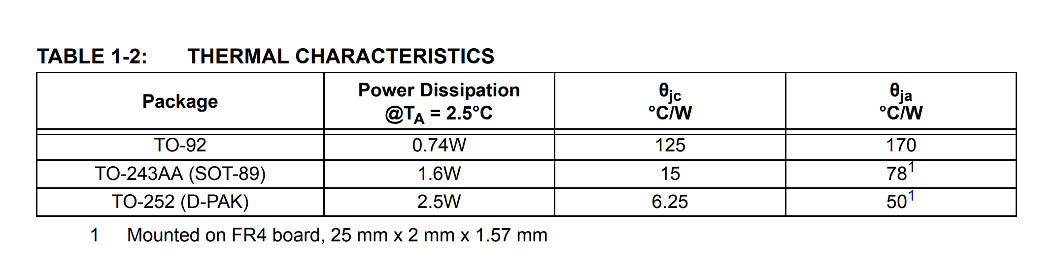
The old package (TO-92) lacked sufficient thermal dissipation, causing the component to overheat and stop functioning. The goal was to dissipate more heat using thermal vias and a copper pour. As seen in Table 1-2, the new package D-PAK dissipated more heat (3.4X) without copper pours or thermal vias.
In Altium Designer, we imported the thermal vias using Altium's Manufacturer Search. The copper pour was implemented to maximize the area of the pour while maintaining distance between the 324V input and VOUT on the regulator.
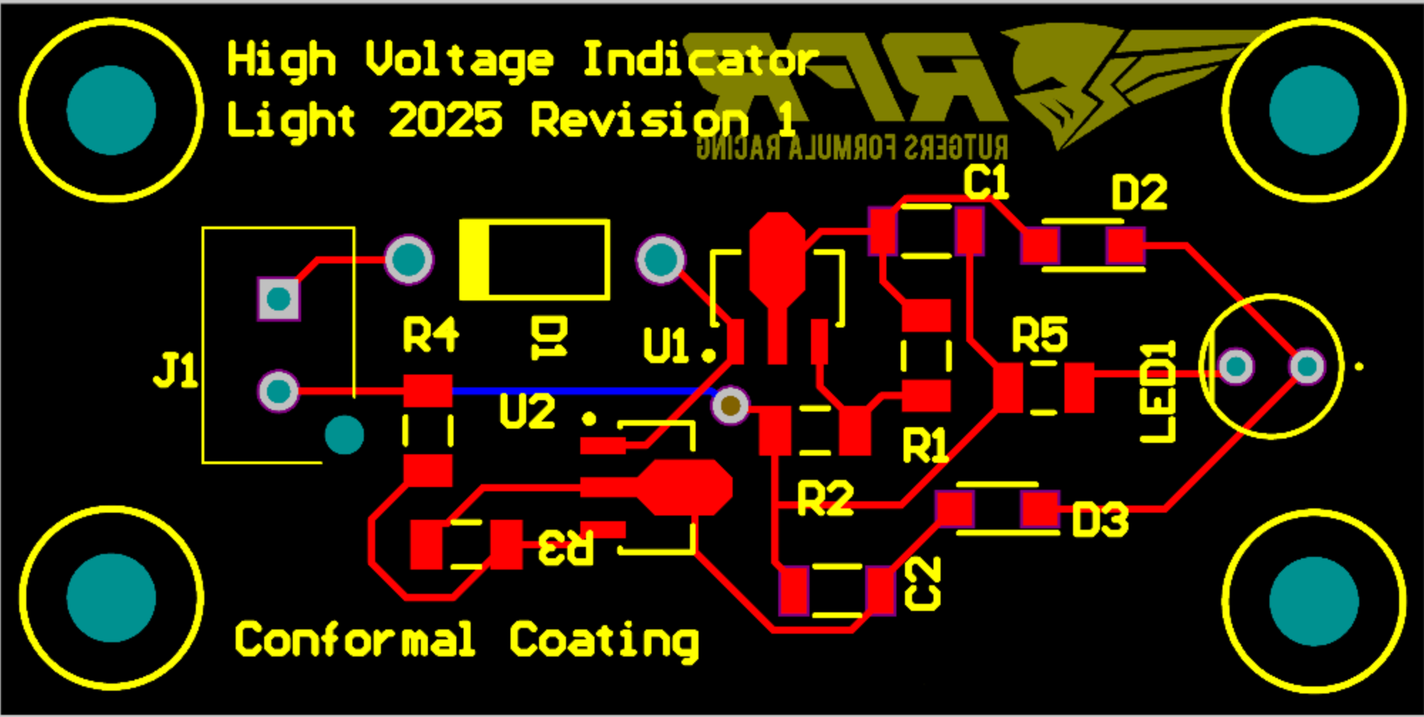
Wired the components so that the PCB was the same size while adding larger components.
Old PCB:
New PCB:
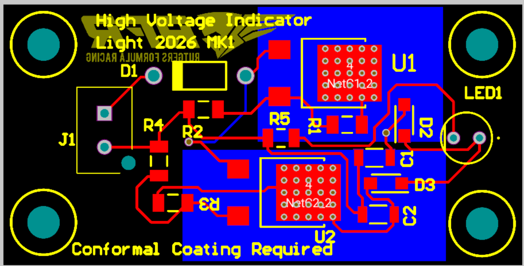
Ran a DRC for JLCPCB specifications and changed the board until everything was manufacturable.