


Design Process
- Component Selection
- Used DigiKey to find a 5V-3.3V IC.
- Selected capacitors and resistors according to the IC's datasheet to regulate and stabilize the input and output voltage.
Part Value / Description Qty Digikey PN LDO IC MIC5366-3.3YC5-TR 1 1865900 Input Capacitor 1µF, 6.3V, X7R, 0603 1 GRM188R70J105KA01DOutput Capacitor 1µF, 6.3V, X7R, 0603 1 GRM188R70J105KA01DPull-up Resistor (EN pin) 10kΩ, 0603 1 RC0603FR-0710KLLED (Optional) Red, 0603 1 LTST-C191KRKTLED Resistor (Optional) 680Ω, 0603 1 RC0603FR-07680RLScrew Terminal (Optional) 2-pin, 3.5mm pitch 1 Phoenix Contact 1935166
2. Symbol and footprint creation.
- Created the LDO footprint using the IPC footprint wizard.
- Added pads according to the documentation
- Linked a 3D STEP model to account for vertical space
- Created a footprint for both IC and connectors.
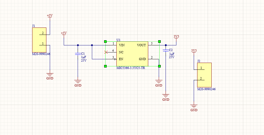
3. Schematic Creation
- Added capacitors to regulate input/output voltage
- Followed WARG guidelines to create an organized, readable schematic
4. Layout
- Placed capacitors close to the IC to reduce resistance.
- Added ground pours on top and bottom layers connected with stitching vias to reduce resistance to ground.
- Added 15mm traces to the board to ensure thermal efficiency.